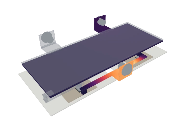
The still image shows the default case. Use the plan view or the 3D model for the current field.
Temperature°C
70.0114.6
FEM-surrogate field (POD reconstruction) interpolated on display lattice points.
Geometry 1:1. The cutaway is a horizontal section below the laminated plates, exposing the AC link and the N riser strap.
Drag / arrows to orbit · Scroll / +/- to zoom · Home to reset · Select a conductorDrag to rotate · Pinch to zoom · Tap a conductor to select
The 2D plan view is active. Calculations, conductor selection and the field remain available.
Loss breakdown
10.24 W
Explore parameters
Tmax114.6 °C · 10.24 W · 0.256 mΩ
Rise above 50 K: the model omits the temperature coefficient of resistivity, so actual loss and rise would be higher.
Current is DC or low-frequency RMS. T_sub is the substrate temperature at the soldered pins and also the convection reference.
50A400
40°C100
Thickness t applies to every plate and strap; width b applies to the P feed foot, AC bridge strap and N riser strap. The 40 mm laminated plate width follows L1.
0.5mm3
2mm6
Constant properties. Presets are typical handbook values (σ in MS/m, k in W/(m·K)), not procurement data.
10MS/m60
100W/(m·K)400
One convection coefficient h applies to every exposed surface.
5W/(m²·K)500
These parameters could not be evaluated. Check the values or restore the defaults.
Current path
Topology follows the switching state
DC+ → P layer → S_H → AC link → AC
AC → AC link → substrate 2 → S_L → N layer → DC−
No P-to-N shoot-through (short-circuit) case is calculated.
I / (b·t) = 83.3 A/mm²
Boundary conditions and assumptions
Electrical: the terminal bolt-washer face is the equipotential current inlet; the soldered pin or source-clip faces of the conducting switch are the equipotential return; other surfaces are insulated.
Thermal: every soldered pin and clip face is held at T_sub; other exposed surfaces convect with h to T∞ = T_sub; conduction into external cables is neglected.
The three conductors are solved separately; conduction between them through the insulation film or air is neglected. Dies carry no loss, so clip faces are also held at T_sub.
Geometry is read from the L1 parameter file; when t grows, the layers move up with the L1 interlayer clearances.
R = R_g(t, b) / σP = I² RT − T_sub = I² R_g² Θ(t, b, h/k) / (σ k)
R_g and Θ come from the FEM-trained surrogate; current, σ and k scale exactly for constant properties.
Conductors
P layerP 层
Role
Distributes current from the DC+ terminal to the high-side substrate drain copper.
Features
Laminated with the N layer across an insulation film to form a low-inductance busbar; soldered to substrate 1 through a feed foot and post.
Common materials
Oxygen-free or electrolytic copper sheet, nickel or tin plated
AC linkAC 连接片
Role
Joins the high-side sources, the low-side drain and the AC terminal to form the half-bridge midpoint.
Features
A collector bar rests on the four high-side source clips and a narrow bridge strap reaches the substrate 2 drain copper; it carries load current in both switching states.
Common materials
Stamped copper strip or copper alloy, nickel plated
N layerN 层
Role
Collects the low-side source current and returns it to the DC− terminal.
Features
Its collector bar rises around the P-layer edge through a riser strap to the upper laminated plate.
Common materials
Oxygen-free or electrolytic copper sheet, nickel or tin plated