Back to work

L6 · 3D teardown

1-in-1 I-type NPC three-level SiC module

One three-level phase leg: a laminated busbar with bent legs onto the dies, copper clips linking T1 to T4, clamp diodes to the neutral point.

Drag to rotate · Scroll to zoom · Click a part for detailsDrag to rotate · Pinch to zoom · Tap a part for details
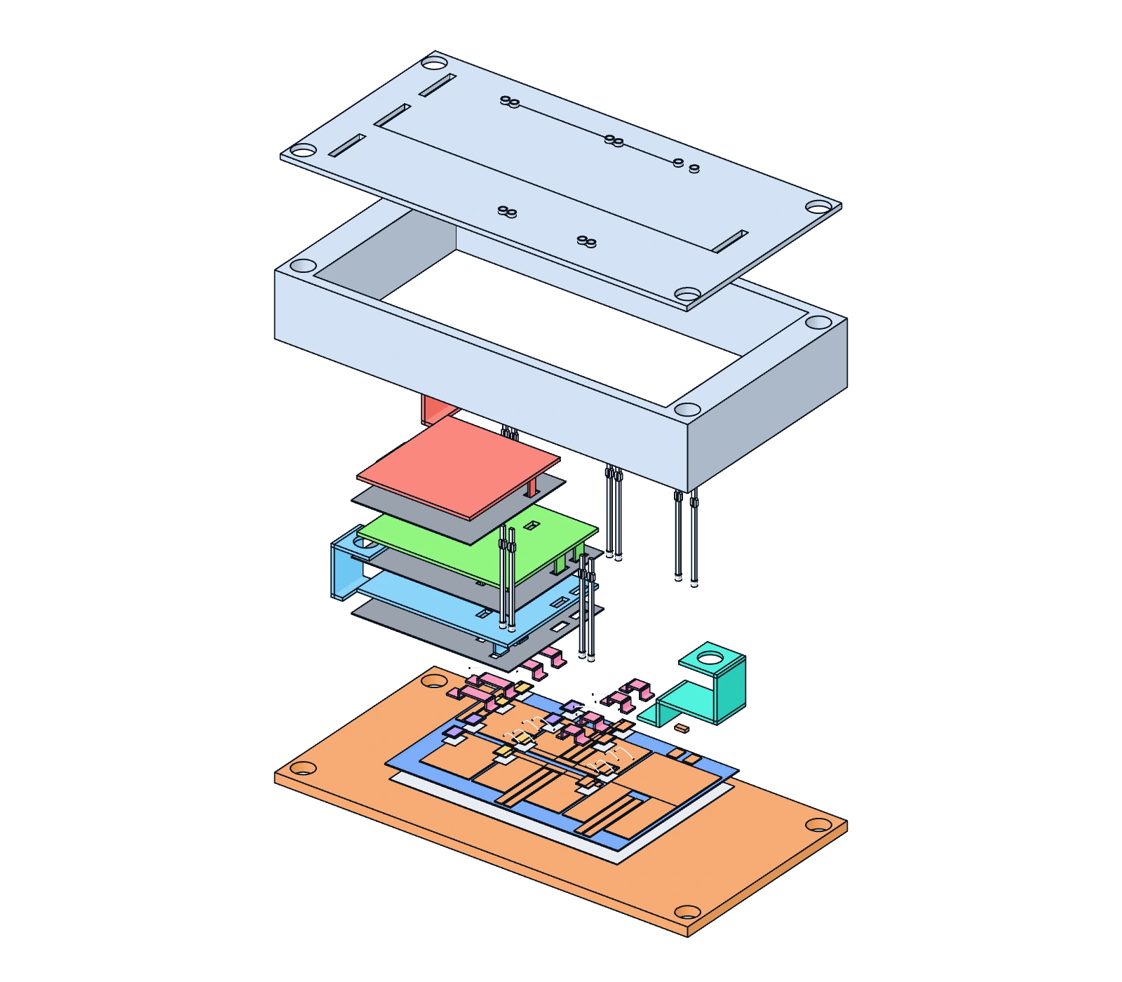
Original 1-in-1 I-type NPC three-level SiC module, exploded: baseplate, AMB substrate, six die groups, copper clips, bond wires, P / NP / N laminated busbar with films, AC terminal, press-fit pins, housing and lid.

Selected part T1 / T4 outer switches

Switch with PWM, connecting X1 to P and X2 to N.

The image keeps the default explosion; the 2D layer diagram follows separation and selection

AssembledExploded

Separation changes display spacing only. It does not simulate switching, current or manufacturing tolerance.

Keyboard controls

Arrow keys orbit, plus and minus zoom, Home resets the view. Tab moves between parts and topology nodes; Enter or Space selects. Arrow keys adjust separation.

2D layer schematic

Simplified side view of the module layers. Spacing follows the slider and the selected part is highlighted.

Selected part: T1 / T4 outer switches

Full module: baseplate, housing and lid. P / NP / N terminals sit at the left end, AC at the right; press-fit signal pins pass through the lid.

Preparing the 3D view. Part details, the topology and the separation control are available.

Arrow keys orbit, plus and minus zoom, Home resets the view. Tab moves between parts and topology nodes; Enter or Space selects. Arrow keys adjust separation.

Original generic model · 1-in-1 I-type NPC · no switching animation

Model and system boundaries

Each switch position has two parallel SiC MOSFET dies and each clamp diode two SiC Schottky dies. Dies, islands, clips and legs are simplified blocks and bent strips; fillets, solder menisci, silicone gel and nuts are omitted.

The layout follows the commutation loops: T1 beside D5 and T4 beside D6, with the P / NP / N layers stacked closely to keep the short loops low in stray inductance. Gate and Kelvin-source signals run on narrow substrate traces to press-fit pins.

In an I-type NPC leg each device blocks half the DC-link voltage in steady state, which is why the topology is common in 1500 V solar and storage inverters. No voltage, current or thermal ratings are given here.

Stray inductance, current sharing, temperature and lifetime are not calculated. Listed materials are common categories for understanding each part, not a product bill of materials.

Generic schematic model based on public information, unrelated to any vendor or employer product. The package style follows public 1-in-1 three-level module literature; geometry, dimensions and layout are an original parametric teaching model.